
Pogo Pins and Spring Test Probes: Selecting for the Intended Task
Published on September 21, 2026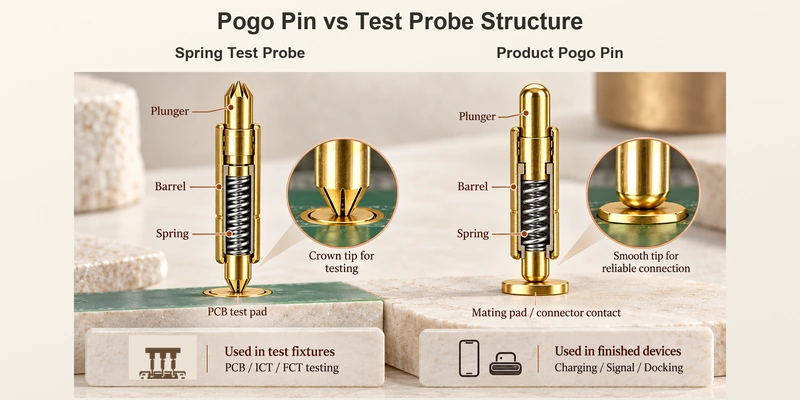
- Overlapping Spring-Contact Terminology
- The Shared Operating Principle
- Product Contacts and Test Probes Compared
- Choosing the Contact Tip
- Applications in Products and Test Fixtures
- Selecting for the Intended Task
- Using a Product Pogo Pin in a Fixture
Pogo pins and spring test probes commonly contain a plunger, barrel and spring. Product contacts are usually integrated into charging and signal interfaces, while test probes are optimized for temporary, repeated contact during PCB testing.
Pogo pinstest probesOverlapping Spring-Contact Terminology
Both belong to the family of spring-loaded electrical contacts, so their names can overlap in use.
A typical spring-contact probe has a plunger, spring and barrel. The spring permits movement and applies a specified force to the target. Designs in this family are used in test systems, fixtures and probe cards, with suitability determined by the selected probe.
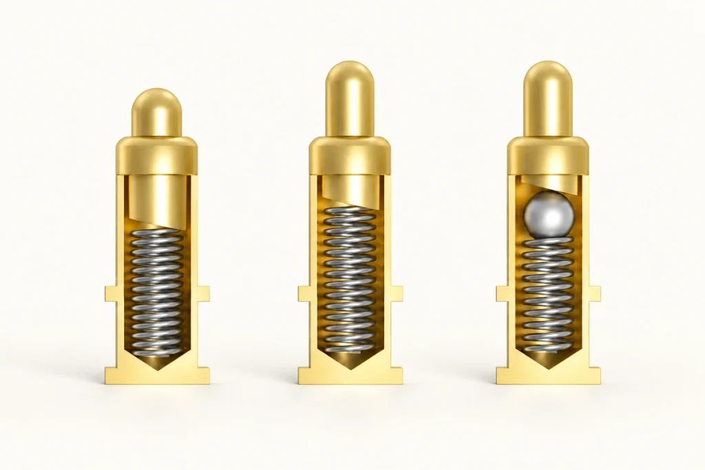
Within PCB test-fixture work, names such as pogo pin, spring-loaded test probe, spring contact, contact pin and test probe may refer to similar components. FixturFab's fixture-selection guidance uses these overlapping terms in that context.
The application provides a useful distinction:
A product pogo pin is usually selected as part of a finished device's electrical interface.
A spring test probe is selected for repeated temporary contact with electronic test points.
Assess the task for which the contact has been optimized when comparing these closely related designs.
The Shared Operating Principle
Spring force in either design supplies the pressure needed for electrical contact.
Touching a pad or test point pushes the plunger into the barrel and compresses the spring. The spring then presses it against the target, allowing limited dimensional variation within the designed stroke and alignment range.
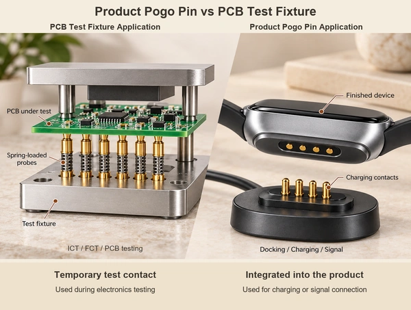
The usual components are:
Plunger: The movable contact that touches the mating surface.
Barrel: The guide and enclosure for the plunger and internal parts.
Spring: The component that supplies contact pressure.
Within its working range, spring travel supports repeatable contact despite small height differences. This ability to accommodate mechanical tolerance is useful in test fixtures.
The shared mechanism needs different tip geometry, mounting, duty cycle, mating surface and specifications for different tasks.
Product Contacts and Test Probes Compared
| Comparison Feature | Product Pogo Pin | Spring Test Probe |
|---|---|---|
| Primary task | Electrical connection within a device | Temporary electrical test contact |
| Typical location | Finished electronic product | Test fixture or system |
| Applications | Charging, docking, batteries, signals and data | ICT, FCT, PCB and component testing |
| Target surface | Mating pad or connector contact | PCB pad, via, terminal or test point |
| Tip geometry | Often flat, rounded or adapted to the product | Crown, spear, needle, serrated, flat, cup and other forms |
| Mounting | PCB, housing or connector assembly | Often a fixture or matched receptacle |
| Selection inputs | Current, stroke, force, pitch, size, plating and exposure | Tip, target surface, force, travel, pitch and cycles |
| Operating environment | May need sealing or corrosion protection | Often a controlled test environment |
Scroll horizontally to view every column.
The main distinction is the design priority.
For a wearable or dock interface, priorities may include compact size, current capacity, resistance, sealing, mating life and corrosion protection.
A production-test probe may prioritize repeatability, target condition, tip shape, fixture pitch, spring force, replacement and test cycles.
Similar mechanisms can therefore have different jobs and selection criteria.
Choosing the Contact Tip
Tip design makes the differing tasks visible.
A product contact generally mates with a defined pad, allowing a flat, rounded or application-specific tip.
Test probes may target solder pads, vias, terminals, component leads or surfaces carrying oxide and flux residue. Different target surfaces call for different tip designs and controlled contact force.
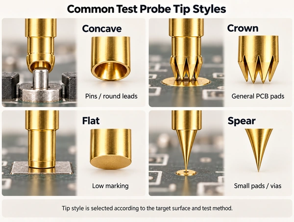
Possible tip styles include:
Crown: Several contact points can suit solder-coated pads and general test points when the force and surface are compatible.
Spear or needle: A small tip concentrates force and may suit a small pad or via, subject to target geometry.
Serrated: Multiple edges can help make contact through certain deposits or oxides; check surface damage and force limits.
Flat: Consider where minimizing marks is important, with suitable pressure and surface condition.
Concave or cup: Can help center a contact on a pin, lead or terminal.
Tip style is a key selection input. Probe suppliers provide crown, spear, serrated, flat and other geometries to match different targets; verify the selected manufacturer's tip description for the actual surface.
Diameter and current rating alone do not identify the correct probe. The target surface is central to choosing its tip.
Applications in Products and Test Fixtures
Product pogo pins can be integrated where a device needs a compact, repeatable electrical interface.
Examples include:
Wearables
- Smart glasses
Medical devices
- Charging docks
Handheld terminals
Battery connections
- Magnetic charging interfaces
Board-to-board connections
Depending on the electrical design, the contacts may carry power, signals, identification or data.
Spring test probes are used for electronic production and testing tasks such as:
PCB testing
- In-circuit testing (ICT)
Functional testing (FCT)
Programming fixtures
Bed-of-nails fixtures
Component testing
Automated production testing
A bed-of-nails fixture places multiple probes on PCB test points at once. Choose geometry, force, current capacity and test-point design together for the board layout.
The operating context helps distinguish the usual use of the two names.
A contact integrated into the finished product is commonly described as a product pogo pin or connector. One primarily used for temporary testing is commonly specified as a spring test probe.
Selecting for the Intended Task
Begin with the contact's expected job.
For a finished-product interface, define:
Rated current
Working stroke
Spring force
Contact pitch
Installation height
Contact resistance
Plating
Required mating cycles
Corrosion protection
Sealing structure
Repeated sweat and moisture exposure in wearables makes plating and corrosion protection important selection inputs.
For a test fixture, ask:
What type of test point must be contacted?
Is the target a pad, via, solder joint, terminal or pin?
Which tip geometry suits it?
What contact pitch is available?
How much spring force can the PCB accept?
How frequently will the fixture operate?
Must the probe be readily replaceable?
Define spring force, travel, tip style, pitch, electrical characteristics and required probe life. Confirm those parameters in the selected supplier's specification.
Select according to the application's electrical, mechanical, environmental and cycle requirements, regardless of the product's label.
Using a Product Pogo Pin in a Fixture
It may be suitable for some applications.
The shared spring-contact principle allows a product pogo pin to make temporary contact with a PCB or another test point.
That capability does not make every product contact suitable for high-volume production testing.
A production fixture may require specific:
Tip geometry
Spring force
Working travel
Compatibility with the selected receptacle
Test-point pitch
Cleaning procedures
Replacement intervals
Performance under high repetitive-cycle use
Receptacle-mounted probes can be replaced after wear without rebuilding the whole fixture. The matched probe-and-receptacle arrangement is therefore important in many production-test designs.
A conventional pogo pin may be adequate for occasional contact or a low-volume custom fixture. For repeated production testing, select a contact for the test method and target surface, including its maintenance requirements.
Choosing by Application and Contact Requirements
Product pogo pins and spring test probes are closely related forms of spring-loaded electrical contact.
Both commonly use a plunger, barrel and spring. Product contacts support charging, signals, battery connections, docking and magnetic interfaces, while test probes prioritize repeatable temporary PCB or electronic test contact.
Use the application requirements to guide selection.
For device interfaces, review current, stroke, force, plating, pitch, environmental protection and mating life. For testing, emphasize tip geometry, target surface, fixture pitch, force, travel and repeated-test requirements.
Frequently Asked Questions
1. Do 'pogo pin' and 'test probe' mean the same thing?
The names can overlap because both may contain a spring-loaded plunger, barrel and spring. Product contacts are usually integrated into devices; test probes are typically optimized for repeated temporary PCB or component-test connections.
2. What does a pogo-pin test probe contact?
It makes temporary electrical contact with PCB test points, pads, vias, terminals or component leads. Uses include ICT, FCT, programming fixtures and production-test fixtures.
3. Why are different tip shapes available?
Crown, spear, flat, serrated and concave tips produce different contact behavior on pads, vias, solder surfaces, terminals and leads. Select the geometry for the target and test method.
4. Which requirements should be specified for a spring test probe?
Specify diameter, pitch, force, working travel, tip geometry, target surface, current, mounting method and expected test cycles.
5. Are pogo pins confined to PCB testing?
No. Finished devices also use them for charging, batteries, docking, signals, data and magnetic interfaces, with capabilities determined by the complete electrical design.