
Magnetic Connector Wiring: Power, Signal Mapping and Validation
Published on August 18, 2026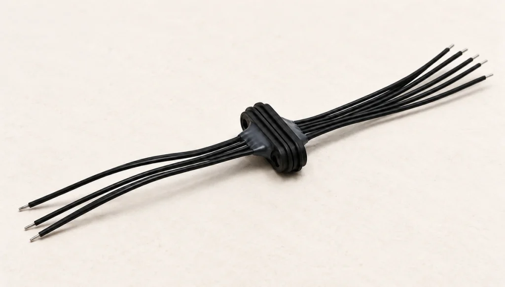
- What the contacts and magnets do
- Defining power, return and signal functions
- Example allocations for different contact counts
- Cable termination and PCB integration
- Checks before connecting the device
- Wiring faults to avoid
- Developing a product-specific pinout
In a magnetic electrical interface, spring contacts carry power and signals while magnets assist mating and retention. Begin wiring with an agreed map of power, return and signal functions on both halves. Check continuity, shorts and polarity with power disconnected before progressing to supply-voltage and operating tests.
Contact count is not a wiring standard. Four-, five- and six-contact assemblies can have different power, ground, data, detection or control assignments according to the device circuit. Confirm the actual mapping rather than copying one from a similar-looking part.
What the contacts and magnets do
The interface separates mechanical guidance from electrical transfer:
magnetic contact assemblyMagnets assist alignment and retain the matching halves.
Conductive contacts connect the assigned power or signal paths.
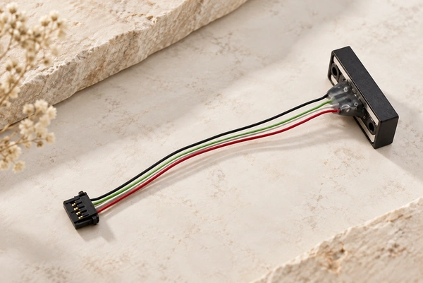
Magnetic attachment normally does not assign electrical functions. Define each contact as the required supply, return, data, detection or other circuit path in the device design.
One possible allocation is shown below:
| Pin | Illustrative assignment | Circuit role |
|---|---|---|
| Pin 1 | V+ | Positive supply path |
| Pin 2 | GND | Power return or ground reference as designed |
| Pin 3 | Signal / Data | Assigned data path |
| Pin 4 | Signal / Data | Second assigned data path |
| Pin 5 | ID / Detect | Identification or mating detection |
| Pin 6 | Control | Charging or device-control function |
Scroll horizontally to view every column.
This table is an example, not a standard pinout. Use the approved drawing and electrical assignment for the exact mating assembly.
For charging with digital data, the complete electrical implementation must meet the intended protocol. USB-IF publishes specifications covering USB interfaces; assigning signal contacts alone does not demonstrate compliance with those requirements.
USB-IF USB 2.0 specification referenceDefining power, return and signal functions
Before terminating wires, document the mapping of both mating halves, including their viewing directions and contact numbering.
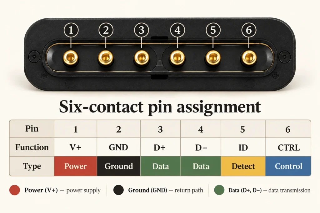
Identify these four function groups:
Positive supply — V+
This path supplies the device. Select the voltage and allowable current for the product, then verify the connector and conductor limits for that load.
Power return or reference — GND
The return completes the supply circuit. It may also provide a signal reference, depending on the circuit; do not assume every isolated or differential interface uses it in the same way.
Signal paths
Other contacts may serve communication, sensors, audio, detection, charging control or auxiliary functions where the device electronics support them.
Detection and reserved contacts
Additional paths can identify the device, detect engagement, enable charging or remain reserved for a defined future function.
A conceptual four-contact allocation for power with USB 2.0-style data is:
| Pin | Illustrative function |
|---|---|
| Pin 1 | V+ |
| Pin 2 | GND |
| Pin 3 | D+ |
| Pin 4 | D− |
Scroll horizontally to view every column.
D+ and D− identify USB data functions, not arbitrary interchangeable lines. An intended USB design needs the applicable electrical implementation and validation. USB-IF publishes the relevant specifications and compliance requirements; this example is not certification or standard USB physical pin numbering.
Approve the contact mapping before PCB layout and cable production. Recording the mating views and polarity helps avoid reversed supply connections, mismatched cable assemblies and orientation errors.
Example allocations for different contact counts
Contact count limits the available paths, but internal connections or parallel contacts can reduce the number of independent circuits. Functions still come from the electrical design.
Two-contact magnetic interface
Two-contact magnetic interfaceA simple two-contact example assigns:
Pin 1 → V+; Pin 2 → GND
Such a layout may suit basic DC supply or charging where no separate signal contact is needed. Confirm the actual supply and protection requirements.
Three-contact magnetic interface
Three-contact magnetic interfaceOne three-contact example assigns:
Pin 1 → V+; Pin 2 → GND; Pin 3 → Signal / Detect
The third path can serve communication, temperature sensing, engagement detection or another low-current function when implemented by the device circuit.
Four-contact magnetic interface
Four-contact magnetic interfaceOne possible power-and-data example assigns:
Pin 1 → V+; Pin 2 → GND; Pin 3 → Data+; Pin 4 → Data−
This allocation can combine power and signals only where the contact design and electronics suit the required protocol. The example does not establish a universal four-contact wiring rule.
Five- or six-contact magnetic interface
five-contactsix-contact magnetic interfaceExtra contacts allow more function choices. A six-contact example is:
Pin 1 → V+; Pin 2 → GND; Pin 3 → Data+; Pin 4 → Data−; Pin 5 → ID / Detect; Pin 6 → Control / Auxiliary Signal
Confirm this example against the actual drawing; it is not a standard six-contact magnetic pinout.
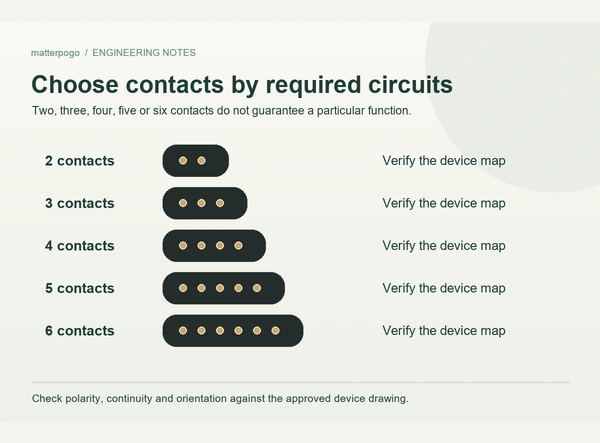
Choose the mapping from:
Device supply voltage and current
Required signal protocol
PCB routing and layout
Cable conductor and construction requirements
Each contact’s allowable current
Signal-integrity requirements
Permitted mating orientation
Applicable safety requirements
Higher-current designs may parallel contacts for supply or return. Evaluate current sharing, contact states and temperature rise; the total allowable current cannot simply be multiplied by the number of parallel pins.
Cable termination and PCB integration
Depending on the assembly, integration may use wire soldering, PCB mounting or a combined connector-and-cable construction. Select a termination supported by the actual part.
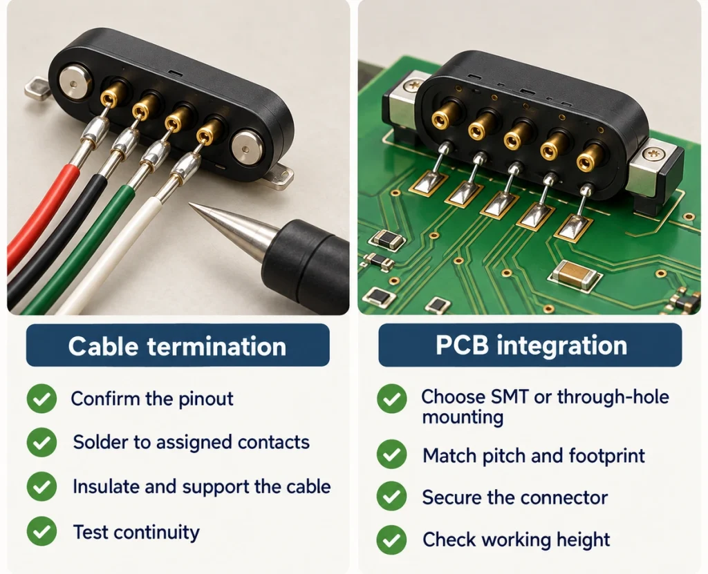
Soldered wire termination
For a cable-side assembly, follow this sequence:
Confirm the approved contact map.
Identify the conductor assigned to each contact.
Prepare the stripped conductor ends.
Solder each conductor to its designated terminal.
Inspect neighbouring terminals for solder bridges.
Provide the required insulation and strain relief.
Check continuity with power disconnected before energizing.
Poor solder joints can add resistance or fail when the cable moves. IPC J-STD-001 addresses soldered electrical and electronic assemblies and can inform the agreed workmanship requirements. The reference does not establish that this connector or its assembly is certified to the standard.
IPC soldered-assembly requirementsBoard-side termination
Depending on the model, board integration may use:
SMT mounting
Through-hole electrical mounting (THT; sometimes labelled DIP)
Solder pads
A product-specific PCB footprint
Match the footprint to the approved pitch, contact positions, orientation and installed working height. Verify the complete mating tolerance stack as well as the solder geometry.
For combined power and signals, review load-current paths alongside sensitive routing. The connector forms part of the electrical interface, so mechanical fit alone is not sufficient.
Checks before connecting the device
Keep the new assembly disconnected from operating power until the initial wiring checks are complete.
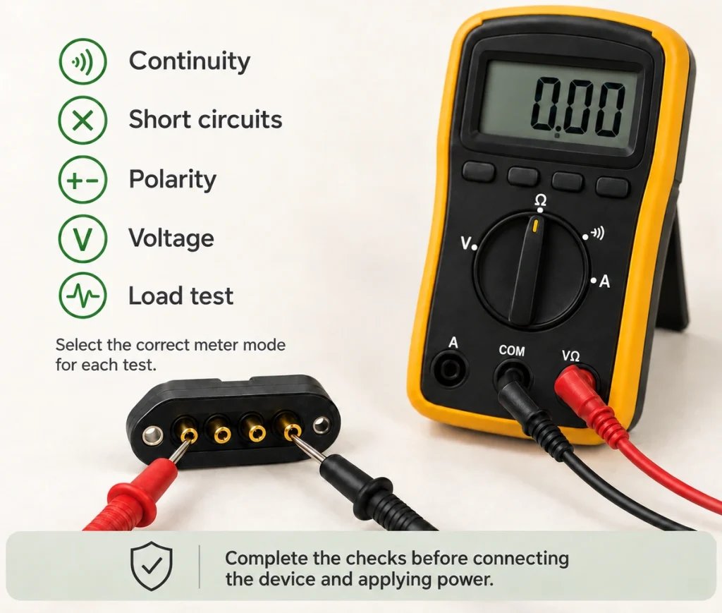
Begin with unpowered electrical checks.
Verify the complete continuity map
With power disconnected, confirm that every contact reaches its intended counterpart. Use the defined views and numbering for both halves, especially where the mating faces appear mirrored.
For a numbering scheme already defined in the drawing, an example is:
Male Pin 1 → Female Pin 1; Male Pin 2 → Female Pin 2
Check every contact, not only the first two.
Look for unintended connections
With power disconnected, verify that the positive path is not unintentionally joined to ground or neighbouring signals.
Small terminal spacing makes careful bridge inspection especially relevant in compact multi-contact assemblies.
Verify polarity in the permitted mating states
Check that the allowed engagement orientations cannot unintentionally exchange the positive supply and return paths.
Mechanical keying, magnet polarity, housing geometry, PCB design and circuit protection can reduce connection errors. Assess the implemented features rather than assuming magnetic attachment guarantees correct polarity.
Confirm supply voltage before attaching the device
After the unpowered checks, energize the supply side in the planned validation setup and measure the contact voltage.
Attach the target device only after the measured voltage and polarity agree with the design.
Validate at the intended operating load
Passing an unpowered continuity check does not demonstrate acceptable performance at operating current. Evaluate the assembled interface under the intended load.
Prototype checks include:
Voltage drop
Contact resistance
Contact-assembly temperature
Stability during charging
Stability of the required signals
Performance over the specified mating duty
A USB implementation also needs the relevant electrical compliance checks. Basic continuity testing does not establish USB compatibility or certification.
Wiring faults to avoid
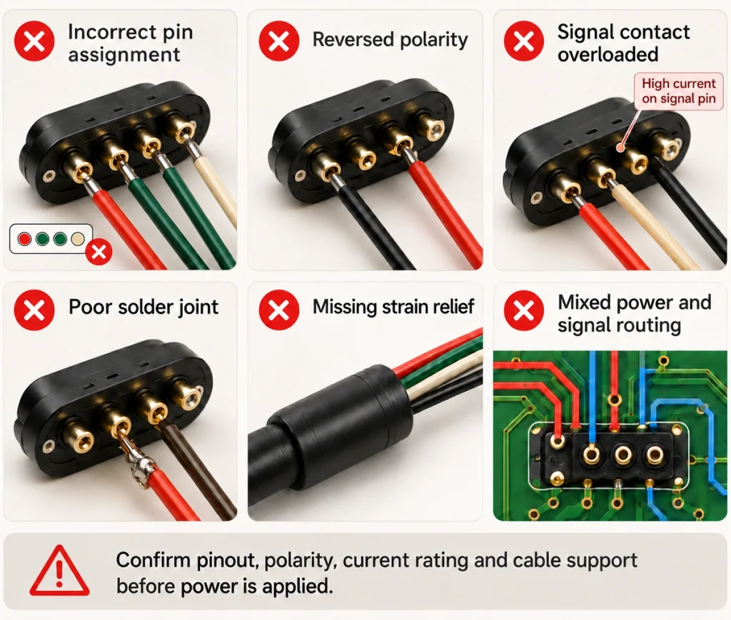
Include these fault mechanisms in the integration review.
Copying a pinout from a different assembly
There is no universal assignment shared by all three-, four-, five- or six-contact magnetic parts. A particular series may have its own approved drawing.
Use that actual drawing to verify every function.
Exchanging supply and return
Reversed polarity can damage the connected circuitry. Specify mating orientation and electrical polarity during design, then validate possible engagement states and protection.
Overloading a contact intended for signals
Contact size, spring structure, plating and resistance influence allowable current. Check each path’s rating and installed thermal behaviour; identical-looking contacts need not have identical load assignments.
Overlooking voltage loss
The contact interface, cable conductors and solder joints all add resistance and voltage drop.
Assess that loss particularly carefully for low-voltage charging at higher current.
Planning power and sensitive-signal routing separately
Develop the contact allocation and PCB routing together when the same interface carries power and data.
Where practical, separate high-current paths from sensitive routing to support the required signal performance and electrical validation.
Treating sealing as a connector-only property
For water, sweat, dust or outdoor use, assess the assembled device. The contact part alone cannot establish the finished product’s ingress or chemical-exposure performance.
The housing, seals, cable exit, adhesive, O-rings and assembly process all contribute to protection. IEC 60529 classifies enclosure ingress protection; specify the required test conditions and validate the assembled configuration. An IP classification does not establish every sweat, corrosion or wet-operation requirement.
IEC ingress-protection classification referenceDeveloping a product-specific pinout
Start with the device’s electrical functions and constraints, then determine the required contacts.
Define the following inputs before selecting or customizing the assembly:
Supply voltage → Current → Power-contact count → Signal-contact count → Signal type → PCB space → Cable exit → Mating orientation → Environmental requirements
Two contacts may suffice for a simple charger. Four, five or six contacts can provide more allocation options where charging, communication and detection are needed together, subject to the actual circuit and connector design.
Magtor can review contact assignments, working height, retention, housing, plating, orientation and cable construction for a custom project. Evaluate these inputs against the existing PCB and enclosure; matching that envelope remains a design and validation task rather than a guarantee of zero device changes.
Wiring review summary
Define the supply, return and signal functions on both halves first. Terminate the cable or board to that map, complete the unpowered continuity, short and polarity checks, then confirm supply voltage before attaching the device. Validate the representative assembly under operating conditions as well.
Contact count and visible position cannot substitute for an approved electrical map. Build the assignment from the application’s functions and requirements, including the mating views, current paths and signals.
Frequently asked questions
How should the wire size be selected?
Select conductor size from the required current, cable length and allowable voltage drop, within the connector and cable limits. Higher-current paths generally need larger conductors than low-current signals. Confirm the complete conductor and contact specifications before approving the wiring.
Can one magnetic interface carry power and data?
It can, where suitable contacts are allocated to supply, return and signals and the complete design supports the required interface. Validate current capacity, signal type, pin assignment and PCB routing together.
Can the contact functions be tailored?
A custom assignment can combine power, ground, data, identification, charging control or auxiliary signals. Agree the mapping and mating views before PCB layout and cable assembly production; customization does not establish support for every protocol.
When is reverse-polarity protection needed?
Where a permitted or foreseeable incorrect mating state could reverse supply and return, assess suitable reverse-polarity protection. Keying, magnet polarity, housing geometry and electronic protection can reduce damage risks, but verify the combined design rather than relying on one feature alone.
What should be checked when data is unstable?
Inspect solder quality, contact resistance, pin mapping, cable length, power interference and signal routing. Check grounding, contact condition and the intended protocol requirements before deciding whether the connector structure needs to change.