
6-Pin Magnetic Connector Pinouts: Functions, Examples and Protection
Published on August 19, 2026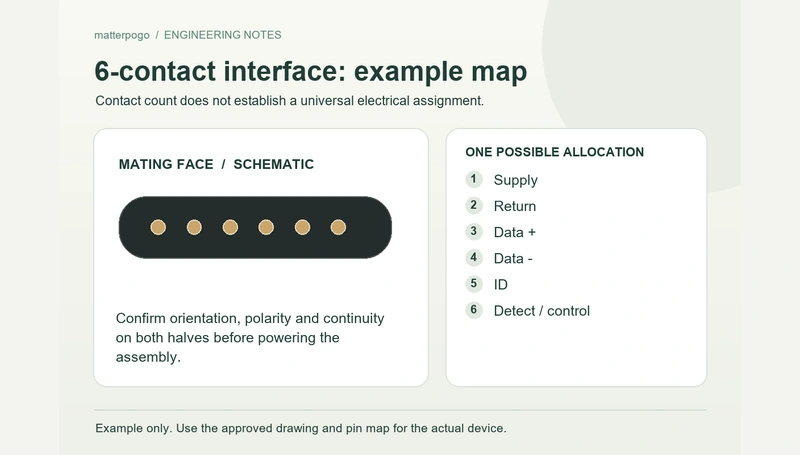
- Why six contacts do not define a standard pinout
- Allocating supply and return paths
- Planning data and other signals
- Identification, detection and control functions
- Five steps for the contact map
- Managing reverse-polarity and shorting risks
- Three illustrative six-contact layouts
- Inputs for a custom interface review
A six-contact magnetic pair has no universal electrical assignment. The device circuit determines which paths serve supply, return, data, identification, detection or control. A power-and-data layout may use V+, GND, Data+, Data−, ID and Detect; another may parallel supply and return contacts. Treat both as design examples, not interchangeable wiring rules.
six-contact magnetic interfaceWhy six contacts do not define a standard pinout
A dedicated six-contact assembly normally follows the product’s electrical design rather than one fixed protocol pin definition. Use the approved mapping for the actual mating pair.
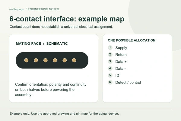
Similar-looking parts can have different functions. One device might allocate four contacts to power and returns and two to signals; another might divide them among power, ground, data, identification and control. Appearance and contact count do not establish compatibility.
Possible functions include:
V+ / positive supply
GND / supply return
Data+
Data−
ID
Engagement detection or a defined control function
Magtor’s wiring guide explains how a multi-contact interface can be assigned around the device circuit. Confirm each function rather than assuming a universal arrangement.
Before connecting unfamiliar equipment, check the approved connector drawing and circuit schematic. Verify the mapping with an unpowered continuity test as appropriate; do not infer it from the visible contacts alone.
The six-contact magnetic connector range provides an entry point for reviewing available configurations and mechanical integration options for a new design.
six-contact magnetic connector rangeAllocating supply and return paths
Establish the supply and return requirements early. They shape allowable current, voltage drop, temperature rise and the necessary protection in the complete circuit.
One low-current example uses a single positive path and return:
| Pin | Illustrative assignment |
|---|---|
| Pin 1 | V+ |
| Pin 2 | GND |
| Pin 3 | Signal 1 |
| Pin 4 | Signal 2 |
| Pin 5 | ID |
| Pin 6 | Detect |
Scroll horizontally to view every column.
Where more conductive paths are needed, another example allocates additional contacts to supply and return:
| Pin | Illustrative assignment |
|---|---|
| Pin 1 | V+ |
| Pin 2 | V+ |
| Pin 3 | GND |
| Pin 4 | GND |
| Pin 5 | Signal 1 |
| Pin 6 | Signal 2 |
Scroll horizontally to view every column.
Parallel paths may support the required power circuit, but do not automatically double a contact rating. Current sharing depends on contact resistance, pin characteristics, PCB traces, cable conductors, compression and the tolerance between contacts. Validate the assembled configuration under load.
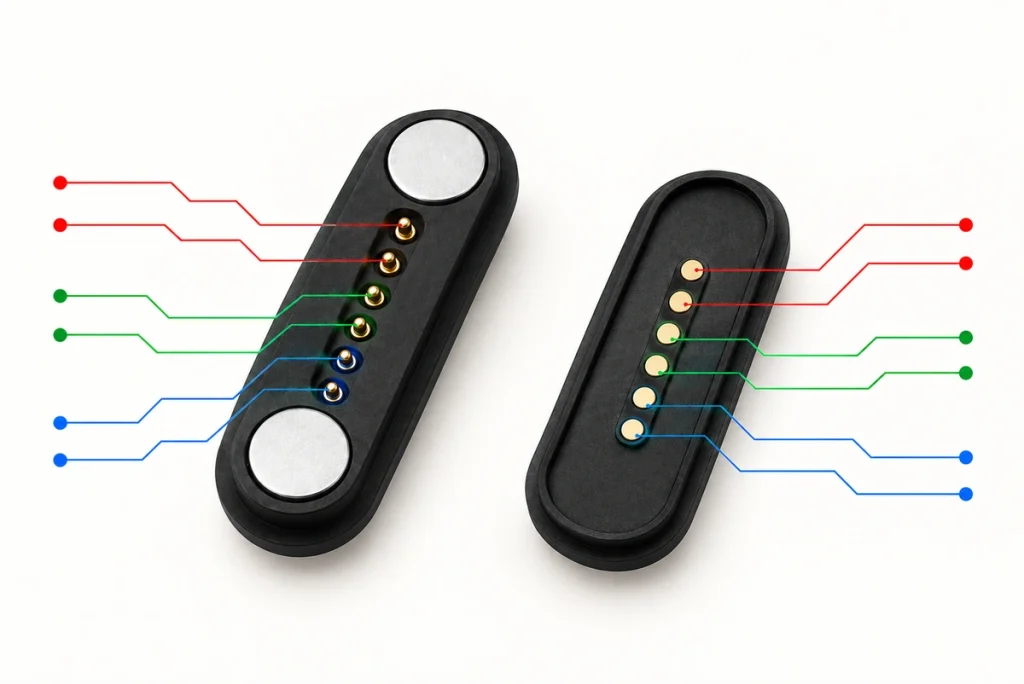
Assess every part of the power route:
Power source → Cable → Magnetic contact interface → PCB trace → Load
Resistance anywhere along that route adds voltage drop and heating. Include the contacts, conductors and terminations when defining the acceptable loss.
The power-and-signal wiring guide gives a fuller sequence for unpowered continuity checks, polarity review and supply-voltage confirmation.
power-and-signal wiring guidePlanning data and other signals
Contacts not needed for the supply paths may serve digital communication, analog or sensor signals, or other defined device functions. Their suitability depends on the full electrical interface.
One power-and-data example is:
| Pin | Illustrative assignment |
|---|---|
| Pin 1 | V+ |
| Pin 2 | GND |
| Pin 3 | Data+ |
| Pin 4 | Data− |
| Pin 5 | ID |
| Pin 6 | Detect |
Scroll horizontally to view every column.
A dedicated serial interface could instead allocate:
V+ | GND | TX | RX | Control | Detect
Six conductive paths do not establish USB, UART, I²C or sensor-protocol support. The electronics, signal levels, return paths, cable and contact arrangement must be designed together for the intended communication.
USB 2.0 uses a D+ and D− data pair with defined signalling and electrical requirements. A magnetic assembly intended in that path needs suitable PCB routing, conductors, contacts, impedance and complete-interface validation against the applicable USB specification.
USB-IF USB 2.0 specification referenceNaming two contacts D+ and D− is not evidence that the interface meets USB requirements.
For sensitive or higher-speed signals, review:
Contact resistance
Spacing between contacts
Board routing
Conductor and cable construction
Differential-pair routing
Signal return and ground reference
EMI
Crosstalk
Geometry of the connector transition
Stability of mating contact
These interconnect details become increasingly significant as signal speed rises.
Identification, detection and control functions
Additional contacts can support functions beyond a basic charging path where the device needs them. Whether six contacts are useful depends on the application’s actual function count.
An identification path can indicate the connected device or accessory. The circuit may use a resistor value, a logic state, a controller or another dedicated scheme; there is no universal ID level implied by the contact name.
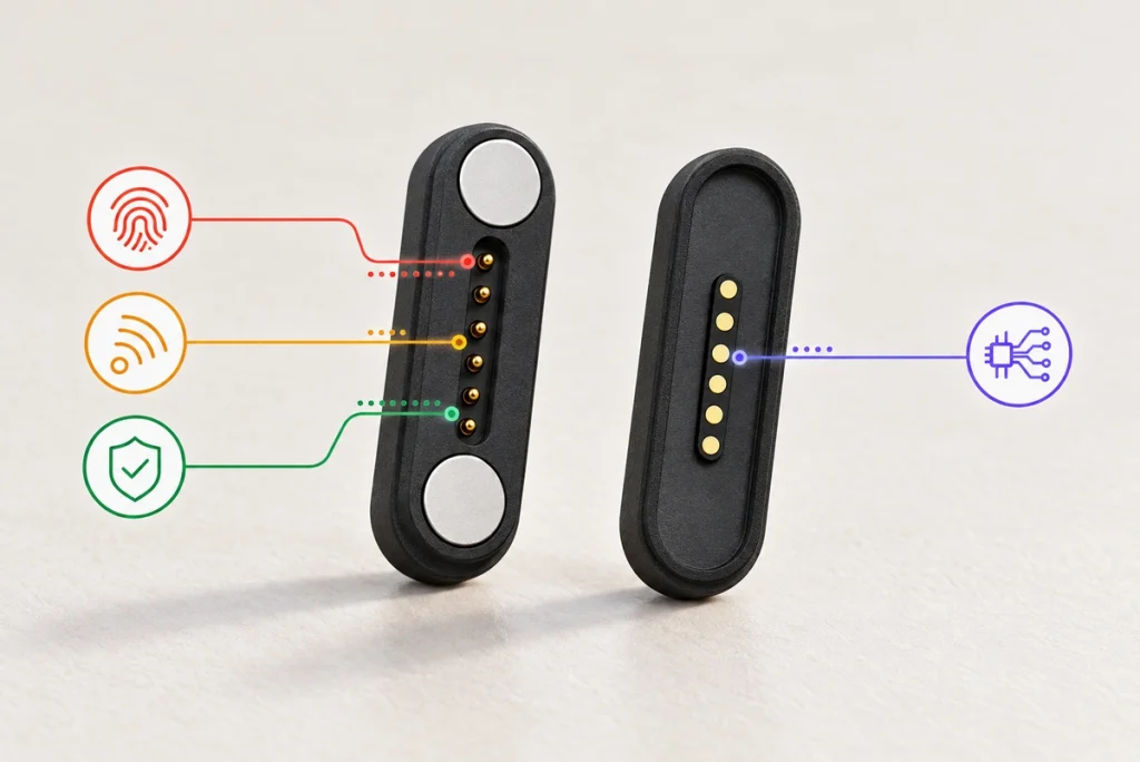
An engagement-detection path can indicate that the joint has docked before charging or communication is enabled, where the required detection logic and timing are implemented.
A control path may support:
Charging enable control
Detection of a docking position
Identification of an accessory
Wake-up signalling
Operating-mode selection
Sensor connection detection
Peripheral control signalling
An illustrative allocation is:
| Pin | Illustrative function | Circuit role |
|---|---|---|
| 1 | V+ | Positive supply |
| 2 | GND | Supply return |
| 3 | Data+ | Defined data path |
| 4 | Data− | Defined data path |
| 5 | ID | Accessory-identification function |
| 6 | Detect | Mating-detection function |
Scroll horizontally to view every column.
Docks, wearables, medical devices, smart products and dedicated accessories may need identification and engagement information before supplying power. This layout is an example for such functions, not evidence of medical approval or compatibility with a particular accessory.
ID and Detect describe roles rather than standardized electrical values. Define the voltage levels, logic states and timing in the device circuit.
Five steps for the contact map
Build the allocation from the system requirements before assigning contact numbers.
1. Specify the power conditions
Record these supply inputs:
Required operating voltage
Maximum continuous load current
Peak load current
Permitted voltage drop
Permitted temperature rise
Use those inputs to assess a single supply path or parallel contacts, including current sharing and the complete installed thermal behaviour.
2. Identify every required signal
List the paths the interface must provide:
Power
Ground
Data
TX / RX
Sensor signalling
ID
Engagement detection
Enable signalling
Control
Then check whether six contacts provide enough paths, including all necessary returns.
3. Plan power and sensitive-signal placement together
High-current paths can introduce noise and voltage disturbances. Allocate and route sensitive data or sensor paths with the required signal integrity in mind.
Review how the proposed contact order reaches the PCB. An allocation that is logical on paper may be difficult to implement if it forces unnecessary crossings or poor routing.
4. Assess the permitted mating directions
Some magnetic geometries can approach from more than one direction. That physical possibility does not mean every orientation is electrically acceptable.
Include this question in the review:
What electrical connections could form after a 180° rotation?
If the first contact can meet the sixth, verify that supply cannot connect directly to ground or energize a sensitive signal unexpectedly. None of the example tables is automatically safe when reversed.
5. Review powered engagement and removal
If the product may dock while its source is energized, include that operating state in the protection review.
Connecting a capacitive load to an energized source can create inrush current. Suitable hot-swap circuitry can manage that event and associated electrical stress. Analog Devices’ guidance explains the design considerations; it does not make the contact assembly inherently hot-plug protected.
powered-engagement circuit protection guidanceFor repeated powered docking, consider:
Inrush-current limiting
Supply-output enable timing
Short-circuit protection
Overcurrent protection
Reverse-current protection
Order of contact engagement
Resolve these circuit and sequencing requirements before approving the contact allocation.
Managing reverse-polarity and shorting risks
Assess incorrect supply polarity as a defined fault case in a magnetic interface.
The magnetic pair can attract even when the electrical order is unsuitable. Develop magnet polarity, housing geometry and contact assignments together.
Possible risk controls include:
Magnetic orientation control
A suitable magnetic arrangement can favour the intended orientation. Verify its effectiveness through the permitted approach and partial-mating conditions.
This can provide a mechanical layer of risk reduction, rather than complete circuit protection.
Asymmetric mating geometry
An asymmetric housing or contact pattern may prevent full engagement after a 180° rotation. Confirm the actual contact states during partial and incorrect approaches.
That approach can help where supply and return locations are not electrically symmetric.
Electrical symmetry where appropriate
An alternative is an allocation that avoids an unsafe supply-to-return connection when the joint is reversed. It requires a compatible complete circuit design.
Some dedicated two-way interfaces place supply or return functions symmetrically, where the mechanical design permits both orientations.
Assess the required signal count and circuit architecture before adopting that arrangement.
Circuit protection against reversed supply
Mechanical controls may need to be supported by electrical protection.
Reverse-polarity circuits can complement mechanical safeguards. TI’s reverse-current and battery-protection discussion covers mechanical and electronic approaches, with topology-dependent losses and behaviour. Reverse-polarity protection is not automatically protection against every other fault.
TI reverse-current and battery-protection discussionDepending on the circuit, options to evaluate include:
MOSFET reverse-polarity protection
Ideal-diode circuits
Current limiting
A fuse or suitable resettable protection device
Overvoltage protection
Input protection ICs
Review orientation, magnet polarity, contact assignments and electrical protection as one system. Validate the relevant fault conditions rather than treating any one measure as a guarantee.
Three illustrative six-contact layouts
The following allocations are starting points for different requirements. Final mapping comes from the actual circuit and approved mating views.
Example A — Parallel power paths with two signals
| Pin | Illustrative function |
|---|---|
| 1 | V+ |
| 2 | V+ |
| 3 | GND |
| 4 | GND |
| 5 | Signal 1 |
| 6 | Signal 2 |
Scroll horizontally to view every column.
Possible use: A charging dock or device needing more power paths than communication paths. Verify current sharing, conductor limits and temperature rise before setting an allowable load.
Example B — Supply, differential data and identification
| Pin | Function |
|---|---|
| 1 | V+ |
| 2 | GND |
| 3 | Data+ |
| 4 | Data− |
| 5 | ID |
| 6 | Detect |
Scroll horizontally to view every column.
Possible use: A dedicated charging and communication interface that also identifies an accessory or detects docking.
Where the pair carries a standardized protocol such as USB, validate the whole interface against its requirements. The table’s labels alone establish no protocol compliance.
Example C — Supply, serial communication and control
| Pin | Illustrative function |
|---|---|
| 1 | V+ |
| 2 | GND |
| 3 | TX |
| 4 | RX |
| 5 | Control |
| 6 | Detect |
Scroll horizontally to view every column.
Possible use: Smart devices, industrial terminals, sensors, docks or dedicated accessories with defined serial levels, direction and control logic.
Choose and validate the final mapping for the device. These examples are not replacement-cable compatibility rules.
Inputs for a custom interface review
Provide the supplier with the following requirements for a custom six-contact assembly:
Required voltage
Continuous and peak load currents
The function assigned to every contact
Communication protocol and signal requirements
Available connector envelope
Board position and mounting constraints
Required working height
Retention and release targets
Permitted mating orientation
Cable length and exit direction
Expected environmental exposure
Required mating-cycle target
For water, sweat or dust exposure, assess contact construction and enclosure sealing together. Magtor’s sealed magnetic connector range can support a configuration review; verify the required ingress and corrosion conditions for the assembled product.
sealed magnetic connector range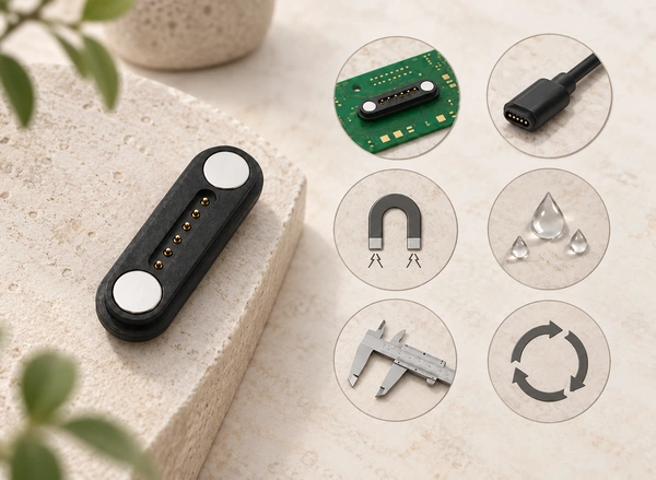
Approve electrical and mechanical details together where possible. A late pinout change can alter PCB routing, conductor mapping, protection circuits and enclosure integration.
Pinout planning summary
A six-contact interface can allocate power, return, data, identification, detection or control according to the product. There is no universal assignment shared by all magnetic six-contact parts.
One illustrative power-and-data allocation is:
V+ | GND | Data+ | Data− | ID | Detect
Another example allocates additional supply paths:
V+ | V+ | GND | GND | Signal | Signal
Select the layout from voltage, current, communication, PCB routing, mating direction and the protection strategy. Validate the complete assembly against those requirements.
For an OEM project, define functions before finalizing the contact order, magnet polarity, working height, retention, housing, cable and mounting. Treat those elements as one interface design.
Magtor’s six-contact magnetic connector range is a starting point for discussing a dedicated power-and-signal assembly and its mechanical requirements.
Magtor