
Specifying Pogo Pin Gold Plating for Wear and Corrosion
Published on August 31, 2026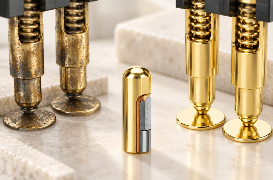
- The Purpose of Gold Plating
- Specifying Plating Thickness
- Selecting Hard or Soft Gold
- How Contact Plating Wears
- Gold Plating and Corrosion
- Assessing ENIG Mating Pads
- Choosing a Plating System for the Product
Gold plating supports a pogo contact's electrical stability, wear performance and corrosion resistance. Select its thickness against mating cycles, spring force, working stroke, gold hardness, pad finish, current and the operating environment.
contact resistanceThe Purpose of Gold Plating
A pogo pin typically contains a plunger, spring and barrel. Its plunger and barrel normally use conductive metal alloys, with a plated outer contact surface to support electrical performance and environmental durability.
pogo pin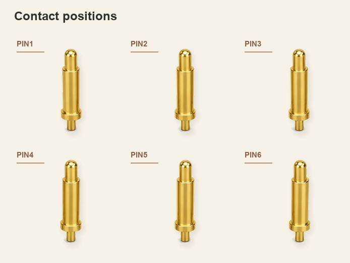
A commonly used layer arrangement is:
Base metal → nickel underlayer → gold contact finish.
Gold resists the formation of insulating surface oxides, which helps preserve a conductive mating surface. This is useful for low-voltage charging, signals and repeated docking.
The nickel underlayer separates the gold from the base material, limits metal diffusion and contributes to the plating system's durability.
Gold primarily protects the electrical contact surface; it does not supply the pin's underlying mechanical strength.
Repeated-use products make this surface function particularly relevant, including:
Examples include wearables, charging docks, hearing devices, medical electronics, handheld terminals, smart products and magnetic charging connectors.
These applications may require the surface to remain functional through thousands of mating cycles.
Specifying Plating Thickness
A single gold plating thickness cannot suit every pogo contact application.
gold plating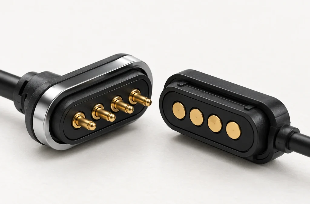
Occasional charging in a clean indoor setting differs from daily sweat exposure in a wearable or an industrial interface expected to handle tens of thousands of cycles. Each may need a different plating system.
The required thickness generally increases when an application demands greater mechanical wear resistance or environmental protection.
A thin gold finish may be sufficient for limited mating cycles in a clean, controlled environment.
More demanding exposure can make a robust plating system important, for example:
Frequent mating, vibration, humidity, sweat, salt, dust, higher contact force or a longer required product life.
Greater thickness alone may not address those requirements.
Contact life also depends on the following factors:
hardness of the gold
nickel underlayer quality
pogo pin tip geometry
spring force
working stroke
alignment
mating pad material
electrical current
environmental exposure
For example, a specification of “0.5 μm gold” cannot be evaluated properly without knowing how the connector will be used. Avoid selecting a contact on that thickness statement alone.
The same thickness can wear at different rates in different products when contact force or lateral movement changes.
Selecting Hard or Soft Gold
Contact finishes commonly use one of two broad gold types: soft gold or hard gold.
High-purity soft gold provides good conductivity and can suit surfaces with little mechanical wear.
Its softness limits resistance to repeated rubbing.
Repeated compression and movement against a pad can wear soft gold more quickly.
Small additions of other elements make hard gold more resistant to wear, so it is generally better suited to repeated mating.
Charging contacts, dock interfaces and magnetic connectors often use hard gold because their contact points undergo repeated compression and small wiping motions.
magnetic connectorsHard gold still does not establish the connector's service life by itself.
Consider a thick hard-gold finish with an offset mechanical layout: the pin may slide sideways over a pad edge on every mating cycle.
That movement can accelerate surface wear despite the finish.
Excess spring force or compression can similarly increase pressure and wear at the contact.
Assess gold hardness alongside the full mechanical design.
The relationship can be summarized this way:
The plating supports surface durability; the mechanical layout controls the forces and movement that wear that surface.
Design the two elements together.
How Contact Plating Wears
Compressing a pogo pin onto its pad applies mechanical pressure between the two surfaces.
Many interfaces also have a small wiping or sliding motion during compression.
Wiping may clear light surface contamination, but the movement also produces friction.
Across thousands of mating cycles, friction can gradually wear away part of the gold layer.
mating cyclesOne possible sequence of wear is:
Repeated mating → friction at the surface → gold wears → nickel is exposed → surface degrades → contact resistance rises.
Wear can be uneven across the contact surface.
The following conditions can make wear faster.
High Contact Force
Additional spring force may improve electrical contact while also raising the pressure and friction between mating surfaces.
The highest available force is therefore not always appropriate.
Choose enough force to maintain contact without exceeding the mechanical limits of the plating and pad.
Working Stroke Outside the Design Range
Use the pin within its designed working stroke.
Minimal compression may leave too little contact force.
Excessive compression may increase mechanical stress and surface wear.
The housing or a mechanical stop should set the final mating position; the pogo pin should not itself stop the moving assembly.
Contact Misalignment
Magnetic interfaces need particular attention to contact alignment.
Magnets can bring the two halves together without guaranteeing that each pin reaches the center of its pad.
Repeated contact at a pad edge can concentrate pressure and add sideways movement, accelerating wear.
Contact Tip Geometry
Flat, dome, crown and other tip shapes distribute contact area and pressure differently.
A small contact area can concentrate pressure.
A larger area may lower pressure but respond differently to contamination.
Match the tip shape to the mating surface and its application.
The Mating Surface
The pin forms only one side of the electrical contact pair.
The pad surface also undergoes wear.
A good gold-plated pin can still perform poorly over time if the pad finish is unsuitable for repeated mechanical mating.
Check this carefully when the mating surface is a PCB pad.
Gold Plating and Corrosion
Gold's chemical stability and resistance to oxidation make it useful on electrical contacts.
An intact gold layer helps separate nickel and the copper alloy beneath it from moisture, oxygen, sweat and other contamination.
That barrier helps keep contact resistance low.
Do not assume the gold layer gives permanent corrosion protection.
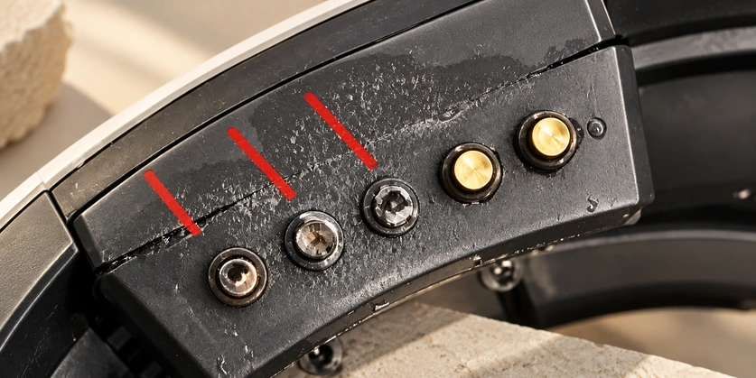
Protection can be compromised when the surface is:
Worn, scratched, porous, contaminated or damaged.
Exposure of nickel or the base material allows moisture and salts to reach more reactive metal layers.
The resulting sequence may be:
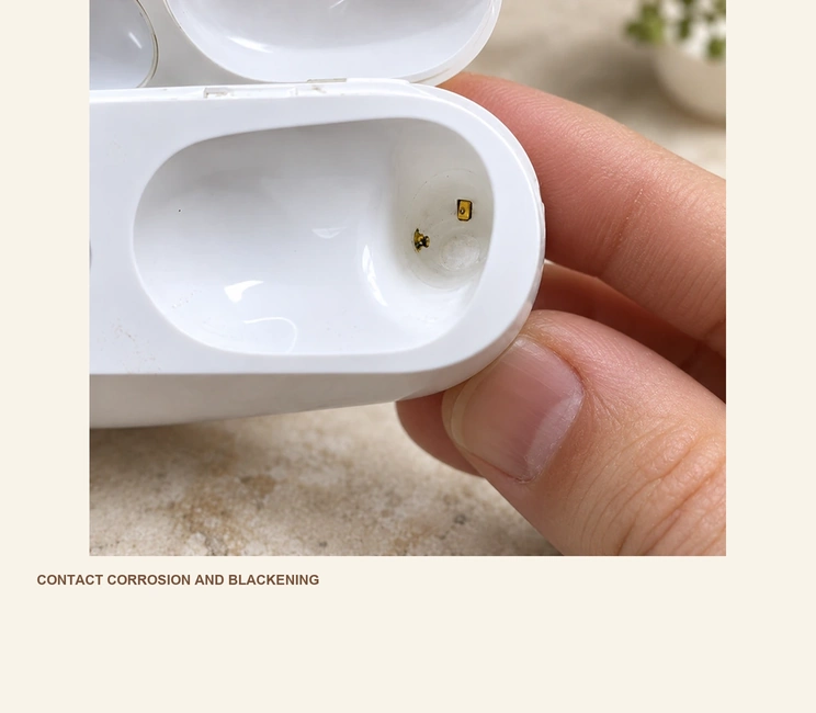
Gold layer damaged → underlying layer exposed → moisture or salt enters → corrosion develops → resistance increases → charging or signals become unstable.
Wearables make this exposure especially relevant.
Their charging contacts may encounter:
Sweat, skin oils, humidity, cosmetics, cleaning agents and repeated handling.
Outdoor or industrial interfaces may also face rain, dust, salt spray, chemicals and temperature cycling.
salt sprayEvaluate plating together with seals, drainage, contact location, housing design and cleaning requirements for these environments.
Water protection at the enclosure does not establish corrosion protection for exposed electrical contacts.
Specify an appropriate surface treatment for the interface itself.
Assessing ENIG Mating Pads
This matters where the pogo pin mates directly to a PCB contact pad.
ENIG means Electroless Nickel Immersion Gold and is a commonly used PCB surface finish.
ENIGENIG provides a flat, solderable surface and protection during PCB manufacture. Its immersion-gold layer is generally much thinner than a dedicated hard-gold finish intended for repeated mechanical contact.
Account for that difference in the contact design.
A pogo pin repeatedly compresses and rubs against the PCB pad.
If the pad finish is too thin for the intended cycle count, the pad may wear before the pin.
Possible effects include:
Higher contact resistance, exposed nickel, surface wear, corrosion or intermittent charging.
ENIG is not excluded from every pogo contact application.
It may be adequate under light load or for relatively few mating cycles.
For high-cycle docks, magnetic connectors, industrial products or equipment intended for years of use, select the pad finish specifically for the expected mechanical wear.
A single-surface check might ask:
“Does the pogo pin have a gold finish?”
The complete-system question is:
“Can both mating surfaces support the required cycle life?”
Assess the pin and pad as a paired contact system.
Choosing a Plating System for the Product
The product's requirements determine its plating specification; a universal thickness value does not.
Begin by defining the intended number of connections.
A contact used a few hundred times has different needs from a dock connected several times daily over a number of years.
Then assess the operating environment.
Clean indoor operation has a relatively low corrosion risk; daily sweat exposure in a wearable can require a more robust contact system.
Include the electrical requirements in that assessment.
Rising contact resistance can increase voltage drop and heating, particularly during charging or high-current applications. Plating condition therefore influences thermal behavior as well as corrosion performance.
high-current applicationsReview the mechanical factors as a group:
Spring force, working stroke, alignment, tip geometry, pad finish and connector structure.
A high-cycle magnetic charging interface, for example, may need:
Wear-resistant pin plating, controlled working stroke, consistent magnetic alignment, a suitable PCB pad finish and environmental validation.
An infrequently connected consumer product may need a different specification.
Also consider the cost of the finish.
Gold adds material cost, and unnecessary thickness on every contact can raise cost without addressing the application's needs.
Specify enough plating for the intended environment and service life, using the application requirements to justify the thickness.
Magtor can configure plating, pin geometry, working height, spring force, magnetic force, cable assembly and connector structure for custom pogo pin or magnetic connector projects, according to the device's mating-cycle and environmental requirements.
MagtorDesigning Both Sides of the Contact
Gold plating influences contact resistance, wear performance and corrosion resistance. Its thickness alone does not determine the reliability of a pogo connector.
The complete system combines these elements:
Base material + nickel underlayer + gold finish + pin geometry + spring force + working stroke + mating pad + operating environment.
Frequent mating gradually wears the gold surface. Once damaged, its protection can be undermined further by sweat, humidity, salt or other contamination that accelerates corrosion.
Select plating with the expected cycles, mechanical design, mating surface, current, environment and product lifetime in view.
For frequent connection or harsh exposure, assess the pogo pin and pad together to support stable contact resistance throughout the intended product life.